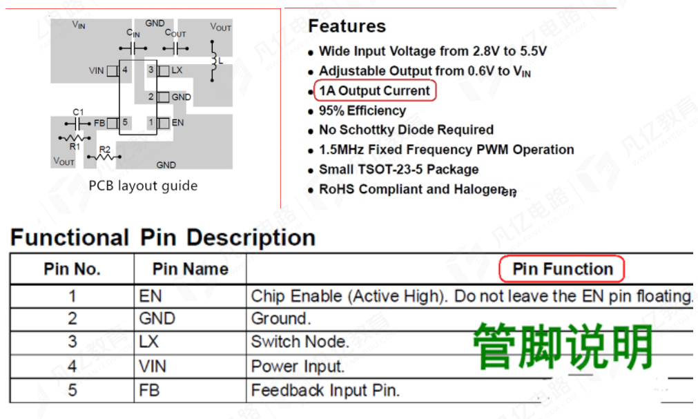
(1) Before the layout, we first need to find the corresponding power IC manual. Generally, the chip manual will contain the most basic power voltage current information and pipe foot information, and Layout Guide. If there is a layout guide, the layout of the layout wiring is performed according to the style inside. Because Layout Guide has been verified by the manufacturer, it can usually make the chip's working status best.
It doesn't matter if there is no Layout Guide. After we understand the power supply and the pipeline information, we can do it according to the conventional requirements of the power supply.
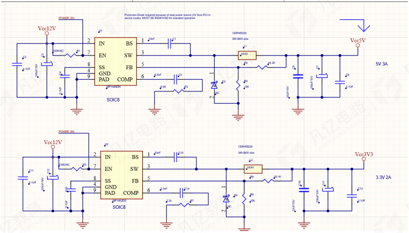
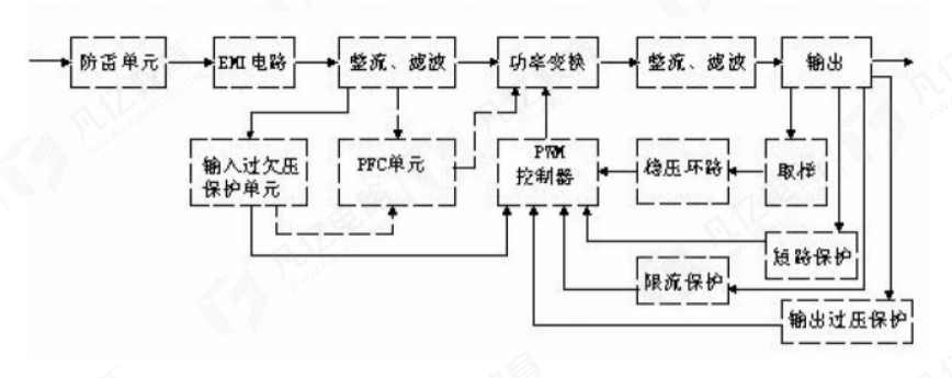
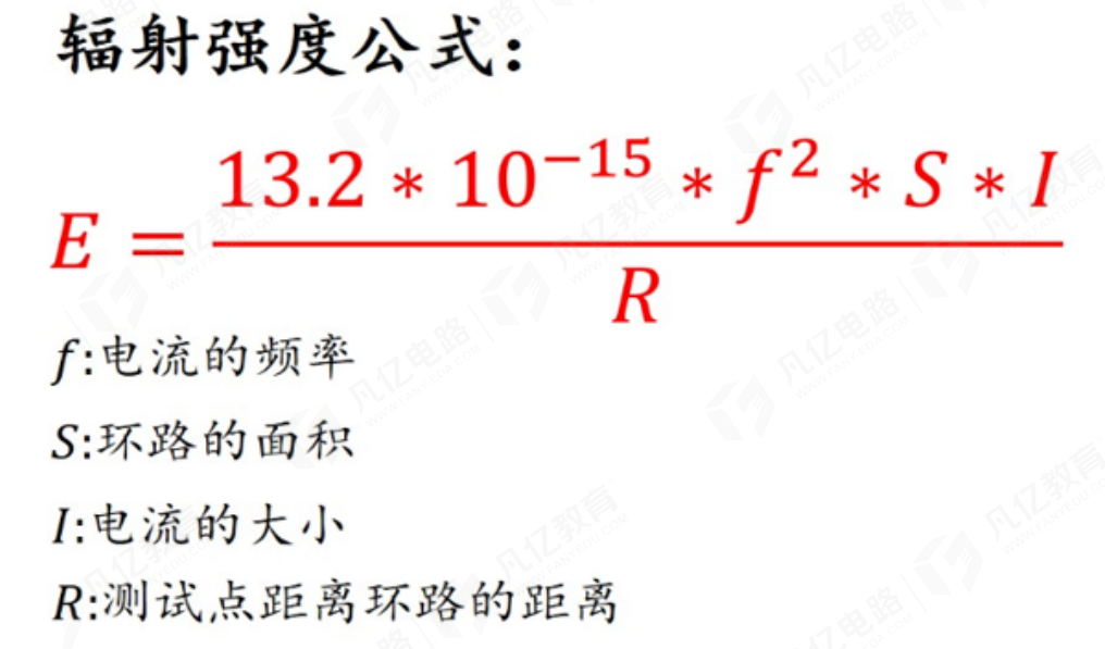
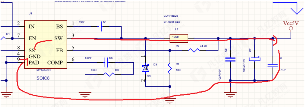
(2) First of all, you need to analyze the input and output of the power supply and the continuation circuit. The smaller the three circuits, the better, because each current ring can be regarded as a loop antenna, which will cause radiation, which will cause EMI problems. Other circuits on the interference board, and the size of the radiation is proportional to the ring area.
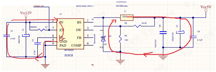
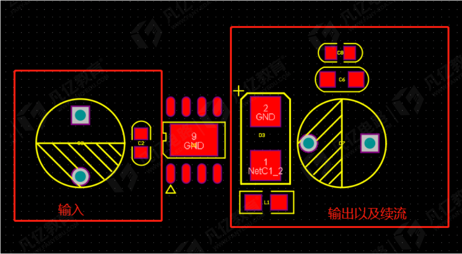
(3) Take out the input and output and the degradation channel first, and other devices can be left without control.
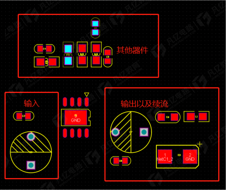
(4) Place the device on the input/output mainway.
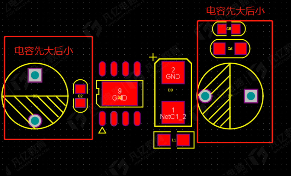
(5) When the filter device needs to be placed reasonably, the filter capacitor keeps the principle of large and then small on the power path.
(6) When placing the device, the device layout is as compact as possible, so that the power path is as short as possible.
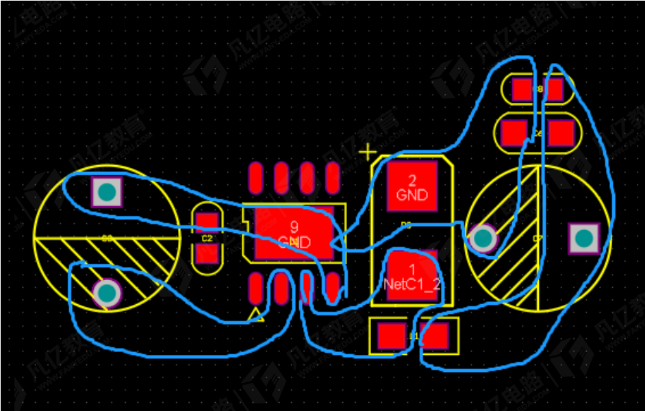
(7) Pay attention to the space for punching and copper to meet the power module input/output channels.
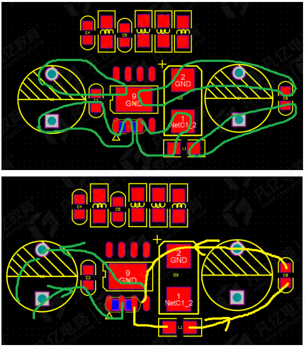
(8) Pay attention to the ring area when layout, and the ring area is small.
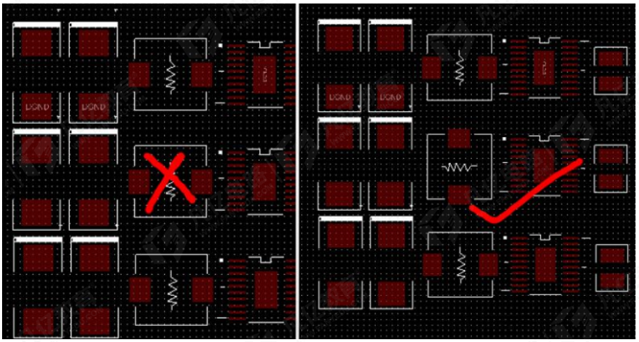
(9) For the switching power supply that outputs multiple roads, try to place vertical placement between adjacent inductors, and large inductors and large capacitors should be arranged on the main device surface as much as possible.
(10) Finally, place the feedback and other devices close to the tube foot.
(11) For a thickness of 1OZ copper, under normal circumstances, 20mil can withstand a current of about 1A; 0.5OZ copper thickness, 40mil can withstand a current of about 1A, and maintain margin when drilling and laying copper.
(12) 0.5mm through-hole overload 1A current - empirical value, evaluation of through-hole size and number, meeting the requirements of current carrying and voltage drop.
(13) The wiring of the power input/output path adopts copper laying treatment, and the width of the copper laying must meet the power supply current size. The input/output path should be minimized by punching holes and changing layers as much as possible.
(14) The position of punching and changing layers must consider the position of the filter element. The input should be punched before the filter element, and the output should be punched after the filter element.
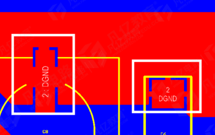
(15) The copper sheet at the copper laying area is connected to the solder pad using a cross connection to reduce welding defects. When the current is particularly high, full connection processing can be used, or copper reinforcement can be applied to the cross to meet the current capacity.
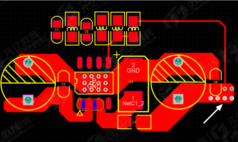
(16) The feedback line needs to be connected to the back of the last filtering capacitor, being careful not to pass through a high current power plane.
(17) After connecting the input and output ground, drill holes on the hot solder pads of the IC fan uniformly.
Source: 21ic official account

Address: Block 2, No. 70, Yaofeng West Road, Wuzhong District, Suzhou City, Jiangsu Province
Tel: 0512-82285066
Email: sales@kegasia.com
Please contact us

WeChat official account
Copyright © Suzhou KEG Industrial Co., Ltd. All right reserved ICP NO: Technical support:Web design